 |
|||
|
|
|||
|
Page Title:
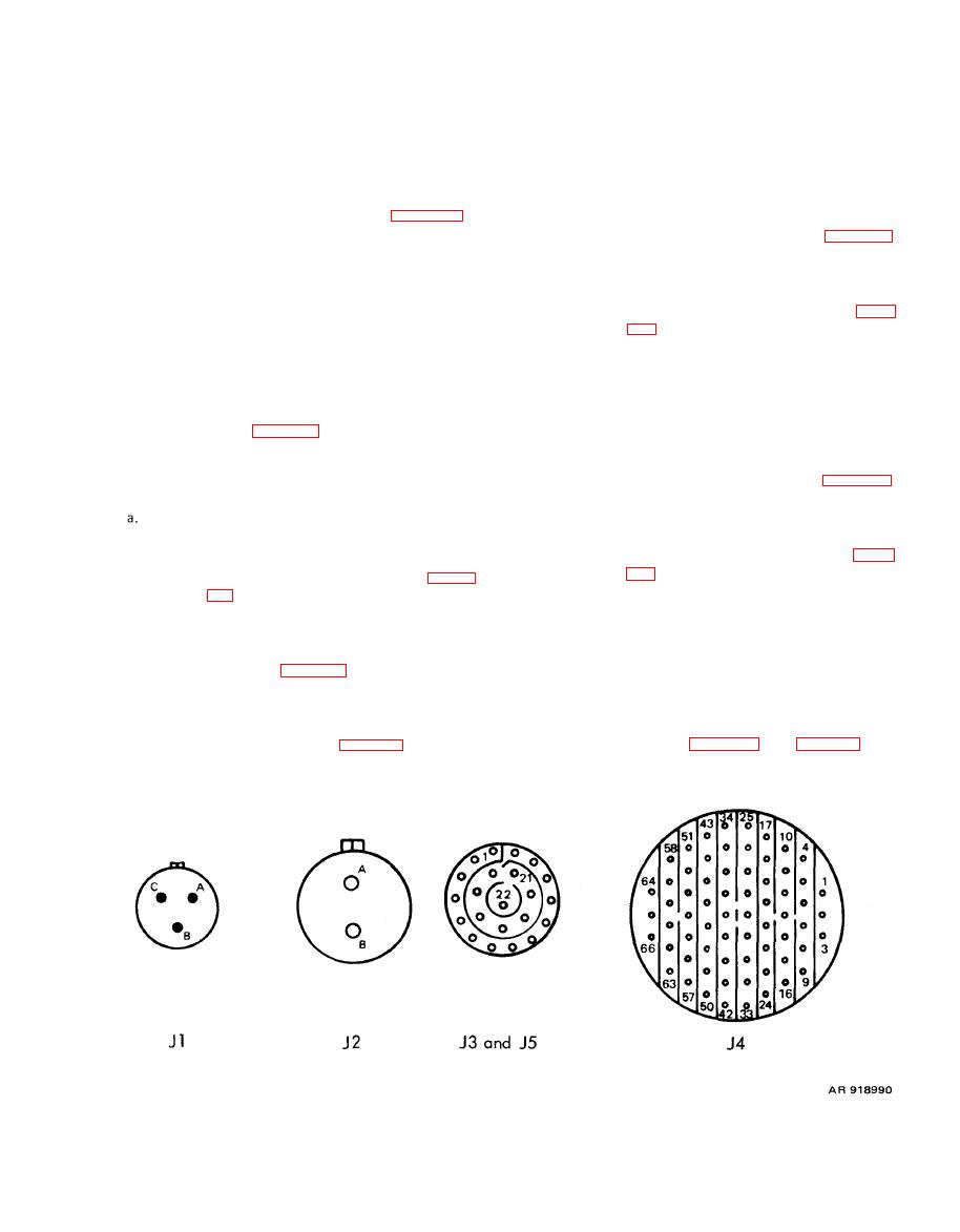
Figure 5-6. Front Panel Connector Pin Patterns |
|
||
| ||||||||||
|
|
 TM 9-4931-378-13&P
b. LAI FLR Switch S3 Wiring Check. Check switch
into two categories: passive (power-off) and active (power-
S3 and associated wiring by performing the follow-
ing procedure:
on), Prior to performing any checkout procedure, remove
the panel/chassis from the enclosure and remove circuit
(1) Connect DVM between TP4 (17) and pin
card assemblies IA I through 1A4 from the card holder on
60 of J4 (36).
the panel chassis. Removal procedures are in Chapter 6 of
(2) Set LAI FLR switch S3 (7) to LAI FLR.
this manual.
(3) Read continuity on DVM. (See table 5-4,
3.)
(4) Set LAI FLR switch S3 (7) to the off
formed with no power applied to the panel/chassis. The
(down) position.
digital multimeter (DVM) is the only test instrument re-
(5) Read open circuit on DVM. (See table
quired for this portion of the checkout. Only continuity
and resistance checks are performed,
c.
A0S
FLR
Switch
S20
Wirinq
Check.
Check
switch S20 and associated wiring by performing
the following procedure:
NOTE
(1) Connect DVM between TP4 (17) and pin
130 of J3 (38).
References to table 5-4 throughout the
( 2 ) Set ADS FLR switch S20 (33) to ADS
following procedures lead to trouble-
FLR.
shooting steps and corrective actions.
(3) Read continuity on DVM. (See table 5-4,
5.)
CPU TEST Switch S2 Wiring Check. C h e c k
(4) Set ADS FLR switch S20 (33) to the off
switch S2 and associated wiring by performing the
(down) position.
following procedure:
(5) Read open circuit on DVM. (See table
(1) Connect DVM between TP4 (17, figure
d. OUTPUT SEL 2 Switch S10 Wiring Check. C h e c k
switch S10 and associated wiring by performing
( 2 ) Set CPU TEST switch S2 (5) to CPU
the following procedure:
TEST.
(1) Connect DVM positive lead to TP7 (14).
(3) Read continuity (less than one Ohm) on
(2) Set OUTPUT SEL 2 switch S10 (12) to
DVM. (See table 5-4,1.)
each of the following positions and read
(4) Set CPU TEST switch S2 (5) to the off
(down) position.
continuity to the designated pin of con-
nector J4 (36). (Pin pattern for J4 is
(5) Read open circuit (more than one meg-
shown in figure 5-6.) (See table 5-4,7.)
ohm) on DVM. (See table 5-4,2.)
|
|
Privacy Statement - Press Release - Copyright Information. - Contact Us |
