 |
|||
|
|
|||
|
Page Title:
Figure 2-2. Bridge Assembly A10, schematic diagram. |
|
||
| ||||||||||
|
|
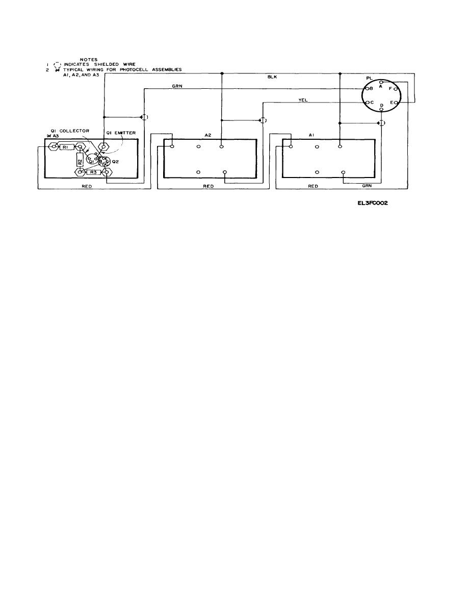 TM 11-6760-238-34
Figure 2-2. Bridge Assembly A10, schematic diagram.
zener diode CR6. Diode rectifiers CR4 and CR5 process
selected light sensitive transistor) diode CR8 is reverse-
ac voltage from transformer T1 through pins U and of
biased and ground is applied through resistors R12 and
connector XA8 to produce full wave pulsating negative
R14 to the base of driver transistor Q2 The action cuts
dc output voltage which is filtered and smooth, by the
off transistor current conduction, applies positive voltage
filter comprised of capacitors C3, C4, and resistor R4.
to the base of transistor Q3 thereby causing transistor
The filtered output voltage is regulated by zener diode
Q3 current conduction Transistor Q3 current conduction
CR6 to a - 6.2-volt dc output and then a piled to terminal
lights SENSOR CAL lamp DS2.
(4) DATA and ELECT FLASH lamp driver
4 of operational amplifiers A1 and A2.
(3) Operational amplifiers and associated
transistors Q4 and Q5 DATA and ELECT FLASH lamp
lamp drivers (The operational amplifiers Al and A2 and
driver transistor stages consist of driver transistors Q4
lamp driver transistors Q2 and Q3 and associated
and Q5 capacitors C5, C6 and associated diodes and
circuitry. When the externally connected SENSOR
resistors. Since both circuits are identical, only the
switch S9 is placed in its CALIBRATED position,
DATA lamp circuitry is discussed.
(a) When the shutter mechanism data request
phototransistor signal energy is coupled through pin of
connector XA8 to the non-inverting input terminal 2 of
switch is actuated, + 28-volt dc power is applied through
operation amplifier Al. In addition, phototransistor signal
pin E of SHUTTER MECHANISM connector J3, diode
energy is applied through pin K of connect XA8 to the
CR20 and resistor R17, charging capacitor C5, and
inverting input terminal 3 of operation amplifier A2.
continues through resistor R19 to the base of lamp driver
When SENSOR switch S9 is in the OPERATE position,
transistor Q4 This action places the transistor in a
ground is applied to input terminal 2 of operational
current conducting state thus flashing DATA lamp
amplifier A1. Operational amplifier A1 and A2 output
A9DS1. The shutter mechanism's DATA pulse however,
signals are applied through diodes CR7 and CR8 to load
is not of sufficient length for the DATA lamp to become
resistor R12 When the operational amplifier output signal
illuminated. After the data pulse is removed, current
is of positive polarity, this signal is applied through the
stored in capacitor C5 discharges through resistor R19
diodes and base load resistor R14 to the base of driver
and the base of transistor Q4 thus holding the DATA
transistor Q2 thus causing transistor conduction. With
Lamp on for a time interval longer than the duration of
Q2 conducting, an effective ground is applied through
the data pulse.
(b) When MASTER switch S3 is set to the LAMP
resist R16 to the base of driver transistor Q3 thus cutting
off the transistor thereby keeping SENSOR CAL lamp
TEST position, a lamp test ground signal is ap-
DS2 from lighting When operational amplifier A2 output
signal is of negative polarity (when light is impinged upon
2-4
|
|
Privacy Statement - Press Release - Copyright Information. - Contact Us |
