 |
|||
|
|
|||
|
Page Title:
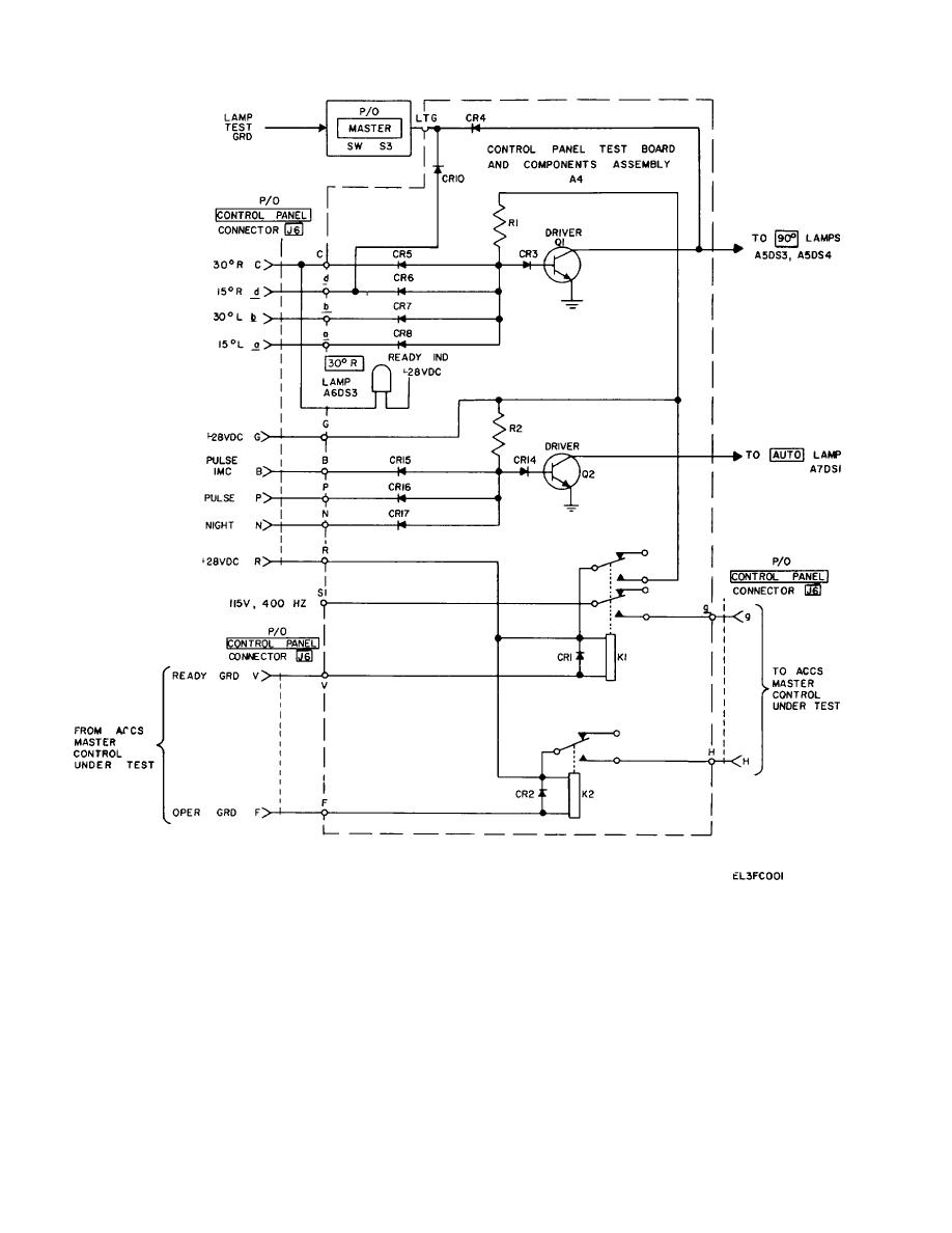
Figure 2-1. Control panel test board and components assembly A4, simplified schematic diagram. |
|
||
| ||||||||||
|
|
 TM 11-6760-238-34
Figure 2-1. Control panel test board and components assembly A4, simplified schematic diagram.
diode CR1. Zener diode CR1 functions to regulate the
CR3 produce + 13-volt dc and + 6.8-volt dc regulated
input + 28-volt dc power to a + 2(0volt dc level which is
outputs respectively. Regulated + 6.8-volt dc output
applied to the base of series regulator transistor Q1
power is applied through variable resistor R6 to voltage
Resistor R1 serves as a zener diode current limiting
divider networks consisting of resistors R7, R8, R10 and
resistor while capacitor C1 functions as a filter capacitor.
R11. Adjustment of variable resistor R6 determines the
Series regulator transistor Q1 produces regulated + 20-
magnitude of positive voltage applied to the voltage
volt dc output which is applied to filter capacitor C2 and
divider networks.
(2) -6.2 V dc power supply. The -6.2-volt dc
zener diode networks comprised of resistors R2, R3 and
diodes CR2, CR3 Resistors R2 and R3 serve as diode
power supply circuitry consists of rectifiers CR4 and
current limiting resistors while zener diodes CR2 and
CR5, capacitors C3 and C4, resistors R4 and R5, and
2-3
|
|
Privacy Statement - Press Release - Copyright Information. - Contact Us |
