 |
|||
|
|
|||
|
Page Title:
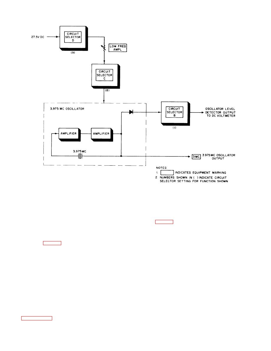
Figure 2-7. 3.975-MHz osillator circuit, functional diagram. |
|
||
| ||||||||||
|
|
 TM
11-6625-467-34
Figure 2-7. 3.975-MHz osillator circuit, functional diagram.
lator circuit).
nects +27.5 volts dc to the HIGH FREQ AMPL con-
trol which adjusts the oscillator output level. In
2-14. 30 MHz Switch Signal Paths.
position 6, CIRCUIT SELECTOR C completes the
path from the HIGH FREQ AMPL control to the 68
The 30 megahertz switch circuit applies a 30 mega-
megahertz oscillator circuit.
hertz signal modulated by a 100 hertz squarewave to
2-13. 500 kHz Switch Signal Paths
the homer module. The signal simulates homer left
and right signals. The 100 hertz oscillator in the
homer module applies the 100 hertz square wave
The 500 kilohertz switch circuit applies a 500 kilo-
modulating signal direct to the switch circuit.
hertz signal modulated by a 100 hertz square wave
Ground applied to either gate input causes a 180
to the homer module. The signal simulates homer
phase reversal of the modulating voltage. In posi-
left and right signals. The 100 hertz oscillator in the
tion 0, CIRCUIT SELECTOR C applies ground to
homer module applies the 100 hertz square wave
m o d u l a t i n g signal direct to the switch circuit.
both the minus and plus gate switch circuit inputs;
in position 1, it grounds the plus gate input, and in
Applying ground to either gate input causes a 180
phase reversal of the modulated output signal. In
position 2, the minus gate input is grounded. The 30
position 3, CIRCUIT SELECTOR C applies ground
megahertz oscillator connects to the switch circuit
to the minus gate input and in position 9, CIRCUIT
through an RF jumper cable connected between the
SELECTOR C grounds the plus gate input. In posi-
30 MC and RF SW IN jacks on the test front panel.
tion 6 or 7, CIRCUIT SELECTOR A connects the
The circuit output appears at the RF SW OUT jack
-
500 kHz fm oscillator to the gate circuit. (Refer to
on the front panel and connects to the homer module
through an RF jumper cable.
2-8
|
|
Privacy Statement - Press Release - Copyright Information. - Contact Us |