 |
|||
|
|
|||
|
Page Title:
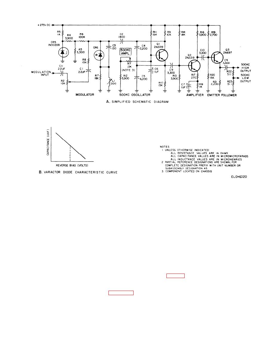
Figure 2-20. 500-kHz fm oscillator circuit, simplified schematic digram. |
|
||
| ||||||||||
|
|
 TM 11-6625-467-34
Figure 2-20. 500-kHz fm oscillator circuit, simplified schematic digram.
CR6 varies the reverse bias of the diode. Since the
quency-modulated signal. The circuit is composed of
diode capacitance is inversely proportional to the
an oscillator, a modulator, an amplifier, and an out-
bias voltage, the oscillator frequency varies around
put emitter follower. The oscillator circuit is an
t h e 500-kHz center frequency at an audio rate.
inductance-capacitance (LC) oscillator composed of
transistor Q1 and associated components. Capaci-
Capacitor C9 couples the 500-kHz oscillator output
to the base of transistor Q2. Transistor Q2 amplifies
the signal and applies it to a voltage divider con-
CR6 form the 500 kHz LC tank circuit. The tank cir-
sisting of resistars R22 and R23. The high-signal out-
cuit connects to the emitter circuit of transistor Q1,
put voltage of the voltage divider applies the fre-
and the feedback path is from the emitter of Q1 to
quency-modulated 500 kHz signal to switches in the
the junction of capacitors C4 and C5. 500 KC AMPL
test set for various module tests. The low-signal out-
control R7 varies the bias on transistor Ql, thereby
controlling the 500-kHz output amplitude. A reverse
put voltage of the voltage divider is applied to the
meter circuit and is used for calibration purposes.
bias voltage is applied to varactor diode CR6 by
Zener diode CR5 (a constant reference voltage de-
2-26. 3.975 MHz and 5.925 MHz Oscillators
vice) in conjunction with voltage divider R3 and R4
through series resistor R6. The capacitance of varac-
tor diode CR6 varies inversely with the voltage im-
The 3.975 MHz and 5.925 MHz oscillator circuits are
p r e s s e d across it. A typical voltage-capacitance
identical except the crystal frequencies are differ-
curve of a varactor diode is given in B, figure 2-20.
ent. For purposes of this discussion, only the 3.975
The modulating signal is applied to the cathode of
MHz oscillator is considered. The oscillator circuit is
CR6 through C11, R2, C1, and R8. Variable resistor
a Colpitts-type crystal oscillator with collector-to-
R2 controls the modulating signal amplitude and
emitter regeneration. Capacitors C2 and C3 form a
thereby controls the deviation sensitivity of the cir-
voltage divider across the oscillator output. The por-
cuit. The modulating signal voltage at the cathode of
tion of the output voltage across C3 is connected to
2-61
|
|
Privacy Statement - Press Release - Copyright Information. - Contact Us |
