 |
|||
|
|
|||
|
Page Title:
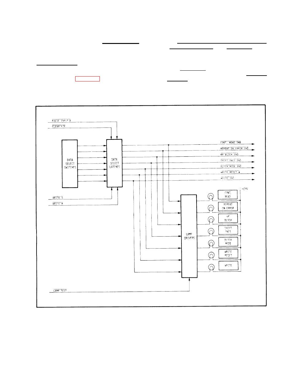
Figure 4-8. Data Control Block Diagram |
|
||
| ||||||||||
|
|
 TM 11-6625-3024-14/EE641-AC-MMA-010/E154 SYSEX/TO 33AA50-5-1-1
The outputs of the Data Select latches are also
provide status inputs to the processor which
include: CONT READ IND, REPEAT ON ERROR
applied to external circuits. 4K BLOCK IND is
IND, BLOCK MODE IND, and WRITE IND.
applied to the Write Data Control circuits to inhibit
the 256-bit counter. This will allow a second
PULSE INPUT 2 from the processor is used to
counter to continue counting to 4096 bits. The
clock the selected switch data into the Data Select
SHIFT ONES IND is applied to the Write Data
Latches. CLEAR F/F signal from the processor
circuits. This signal selects an output from the Data
Word Selector (See Figure 4-3) that will allow ones
clears all latches except the Write Latch. WRITE R
to shift through the eight tracks of data. The
and WRITE S from the processor are used to set or
reset the WRITE latch on command.
remaining outputs from the Data Select Latches
Figure 4-8. Data Control Block Diagram
4-13
|
|
Privacy Statement - Press Release - Copyright Information. - Contact Us |
