 |
|||
|
|
|||
|
Page Title:
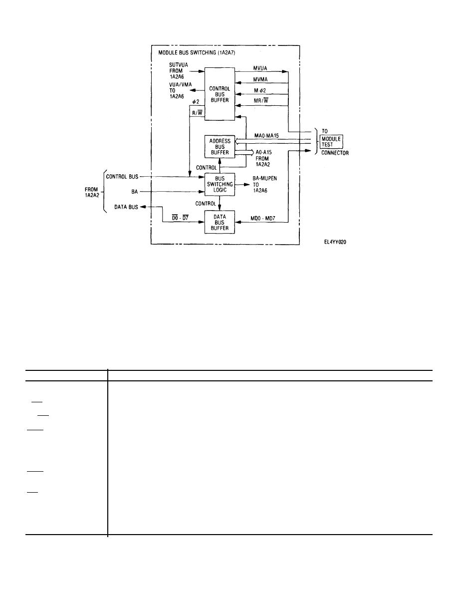
Figure 4-3. Microprocessor block diagram (sheet 3 of 3). |
|
||
| ||||||||||
|
|
 TM 11-6625-2937-13
Figure 4-3. Microprocessor block diagram (sheet 3 of 3).
(1) Basic MPU description. The MPU is an eight-bit word
with its 16-bit address lines. It also contains 128 bytes of
(or byte) microprocessor containing six internal registers
RAM, the first 32 bytes of which can be operated in a low
plus an internal clock oscillator and driver on the same
power mode to prevent the loss of data during power-
chip. Three of the registers are 16-bit (or 2 byte)
down situation. In addition, the eight-bit data bus is
registers, while three are eight-bit (or byte) registers: the
bidirectional as well as three state, which makes direct
16-bit registers are the program counter (PC), the stack
memory addressing and multi-procesing possible. Table
pointer (SP), and the index register ([X). The eight-bit
4-1 lists the various control and data signals normally
registers are accumulator A (ACCA), accumulator B
associated with the MPU.
(ACCB), and condition code register (CCR). This MPU
is also capable of addressing 65 kilobytes of memory
Table 4-1. Typical MPU signal Distribution
Signal
Description
AO-AI5
Address bus 16-bits provide 65 kilobytes of addressing
DO-D7
Data bus Eight bidirectional lines that provide transfer of data to and from the memory and various peripheral
devices.
R/W
Read/write. Output signal informs peripherals and memory devices when the MPU is in a read (high) or write (low)
state. The normal standby state of this signal is read (high). When the MPU is halted, it is in the logical one state.
BA (BA)
Bus available, Normally in low (BA). When activated, it goes to the high state BA, indicating the MPU has
stopped and the address bus is available.
NMI
Non-maskable interrupt. A negative-going edge on this input requests that a NMI sequence be generated within the
MPU. However, the MPU completes the current instruction that is being executed before it recognized the NMI
signal.
XTAK (4.0 MHz CLOCK)
4.0 MHz clock. Triggers an internal oscillator.
VMA (VUA)
Valid memory address. This signal indicates to peripheral devices that there is a valid address on th address bus.
Valid user address (VUA) has the same meaning.
IRQ
Interrupt request. This input requests that an interrupt sequence be generated within the
MPU. The MPU waits until it completes the current instruction that is being executed before it recognized th
request.
RES
Reset. This input is used to reset and start the MPU from a power down conditions, resulting from a power failure or
an initial start-up of the MPU. When this line is low the information in the registers is lost.
02
Phase two clock. This clock signal is used to synchronize the operation of the microprocessing system.
PIT 02
Programmable interval timer phase two clock. This signal synchronizes data transfer between the MPU and the
PIT.
Control Bus
Three pins are used for the control bus. It provides control signals 02, R/W and VMA (VUA).
4-9
|
|
Privacy Statement - Press Release - Copyright Information. - Contact Us |