 |
|||
|
|
|||
|
|
|||
| ||||||||||
|
|
 TM 11-6625-2885-30/NAVAIR 16-35TS3614-2
PRI GENERATION
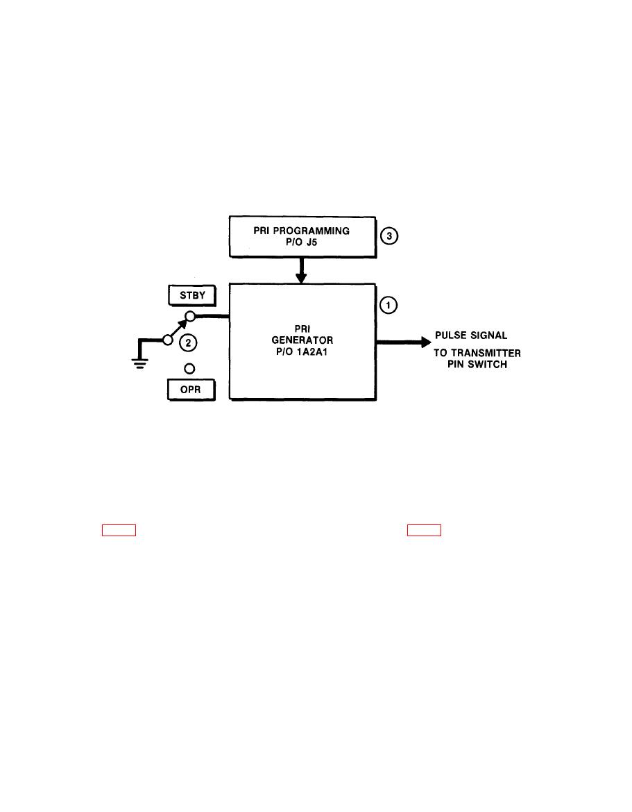
2-6. Circuit card 1A2A1 (1) includes all the PRI generation circuits in the
FLTS. The PRI generator produces a pulse train simulating radar threats, when
STBY/OPR switch (2) is in the OPR position. In the STBY position, no pulses
are generated.
Programming wires (3) on J5 control the PRI and pulse width. The PRI generator
produces pulse pairs which have 100 s separation, at 350 s PRI, and 0.3 s
width.
counters U45, U25, U36 and U37 divide a 10 MHz clock in four decade steps.
Comparators U44, U33, U35 and U47 produce a reset pulse when the decade
count reaches the count wired into' programming pins of the card edge connector.
The reset pulse presets the counter to 0.4 s, to make up for clocked delays.
Decade counter U36 sets flip-flop U17 after a delay of 100 S from reset.
Both the main count and the delayed count supply pulses to dual latch U38.
Decade counters U48 and U49 count out the pulse width wired into proqramming
pins of the card edge connector. Gate U46 controls output pulses which drive a
PIN switch pulse modulator in Transmitter Assembly 1A1.
|
|
Privacy Statement - Press Release - Copyright Information. - Contact Us |