 |
|||
|
|
|||
|
Page Title:
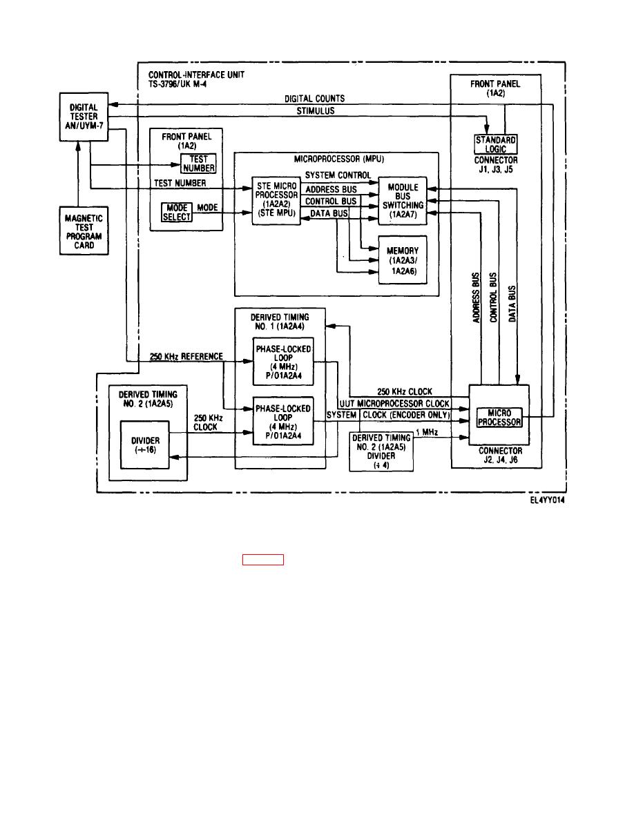
Figure 4-1. Data link tester block diagram. |
|
||
| ||||||||||
|
|
 TM 11-6625-2937-13
Figure 4-1. Data link tester block diagram.
SELECT switch and provides SHORT signal to SHORT
4-2.
Control-Interface Unit Functioning
indicator DS3 (1A2) if the dc voltages selected by the
a. Overall Block Diagram Analysis (fig. 4-2)
MODE SELECT switch for the encoder (5V and 12V)
(1) Power fault detection. The digital tester
or the decoder and STE (+5V and 15V) are not within
provides dc power (+5V +12V/+15V and -12V/-15V) to
the MODULE TEST connector (1A2) and the power
tolerance. The program card inserted in the card reader
supply monitor circuit (1A2A1) via MODE SELECT
slot of the digital tester establishes the correct MODE
switch S2 (1A2). The power supply monitor circuit, in
SELECT switch S2 (1A2) position for the appropriate
turn, monitors the power input from the MODE
MODULE TEST connector (1A2).
4-2
|
|
Privacy Statement - Press Release - Copyright Information. - Contact Us |