 |
|||
|
|
|||
|
Page Title:
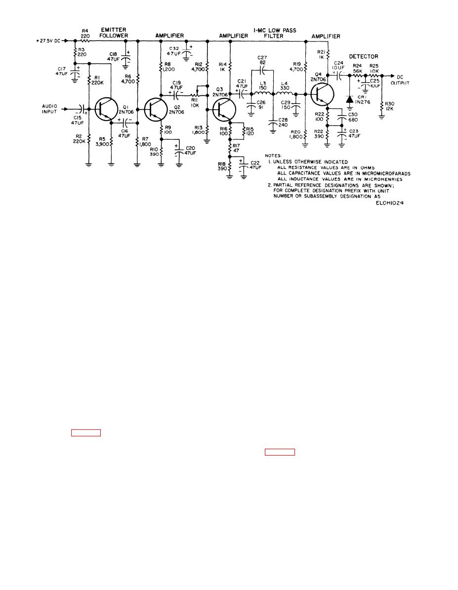
Figure 2-24 Audio amplifier/detector circuit, simplified schematic diagram. |
|
||
| ||||||||||
|
|
 TM 11-6625-467-34
Figure 2-24 Audio amplifier/detector circuit, simplified schematic diagram.
drive at the base of Q3, thereby controlling the gain
of attenuation to the input signal, the 50-ohm input
of the entire circuit. The amplifier circuit of tran-
having the least attenuation and the 500-ohm input
sistor Q3 further amplifies the signal and applies it
h a v i n g the most. Capacitor C9 couples the at-
to the 1-megahertz low pass filter circuit consisting
tenuator output to the base circuit of RF amplifier
of inductors L3 and L4 and capacitors C26, C27, C28,
Q3. The amplifier circuit of transistor Q3 amplifies
and C29. The low pass filter is a two-section pi-type
the RF signal and applies it to the base of transistor
filter with a cutoff frequency of approximately 1
Q2. The amplifier circuit of transistor Q2 further
megahertz. Extraneous signals above 1 megahertz
amplifies the RF signal and applies it to the input of
are attenuated and do not affect the output dc level.
emitter follower Q3. Capacitors C4 and C5 in the
The amplifier circuit of transistor Q4 amplifies the
emitter circuits of transistors Q2 and Q3 are emitter
signal again and applies it to the detector circuit.
peaking capacitors that extend the high-frequency
Resistor R22 and capacitor C30 in the emitter cir-
response of the amplifier circuits. Capacitor C5 is
cuit of Q4 provide frequency compensation to ex-
v a r i a b l e and is adjusted to make the frequency
tend the linear amplification range of the amplifier.
response of the amplifier essentially flat from 3 to 70
The detector circuit is composed of diode CR1, re-
megahertz. The transistor Q1 emitter follower cir-
sistor R24, and capacitor C25. On the positive half
cuit current-amplifies the RF signal and applies it to
cycles, capacitor C25 charges through R24 to a level
the detector circuit. Diode CR1 in the detector cir-
proportional to the peak amplitude of the ac signal
cuit rectifies the RF voltage. A dc voltage propor-
at the collector of Q4. Resistors R25 and R30 form a
tional to the RF input level appears across capacitor
voltage divider. The output of the circuit is taken
C2. Resistors R1 and R4 are meter multiplier resis-
from the junction of R25 and R30.
tors in series with the output to the meter circuit.
Resistor R1 is variable and is adjusted to calibrate
2-30. RF Amplifier/Detector
the circuit.
2-31. 500-kHz Filter
The radio frequency (RF) amplifier/detector circuit
is used in conjunction with the meter circuit to
measure RF signal levels in the test set. The four in-
The 500-kHz filter circuit is composed of three tran-
puts to the amplifier, 50 ohms, 150 ohms, 200 ohms,
sistor amplifier circuits and two 500-kHz filters. The
and 600 ohms, are connected to RF jacks RF VM 1,
circuit may be used as either a wide or narrow band-
RF VM 2, RF VM 3, and RF VM 4, respectively, on
pass filter for checking and adjusting the 500-kHz
the front panel. The four circuit inputs match the
oscillator frequency in the transmit audio module of
different impedances encountered in RF level meas-
Radio Set AN/ARC-54. The wideband mode is used
urements. The inputs also present varying amounts
for go-no-go testing of the 500-kHz oscillator, and
2-65
|
|
Privacy Statement - Press Release - Copyright Information. - Contact Us |
