 |
|||
|
|
|||
|
Page Title:
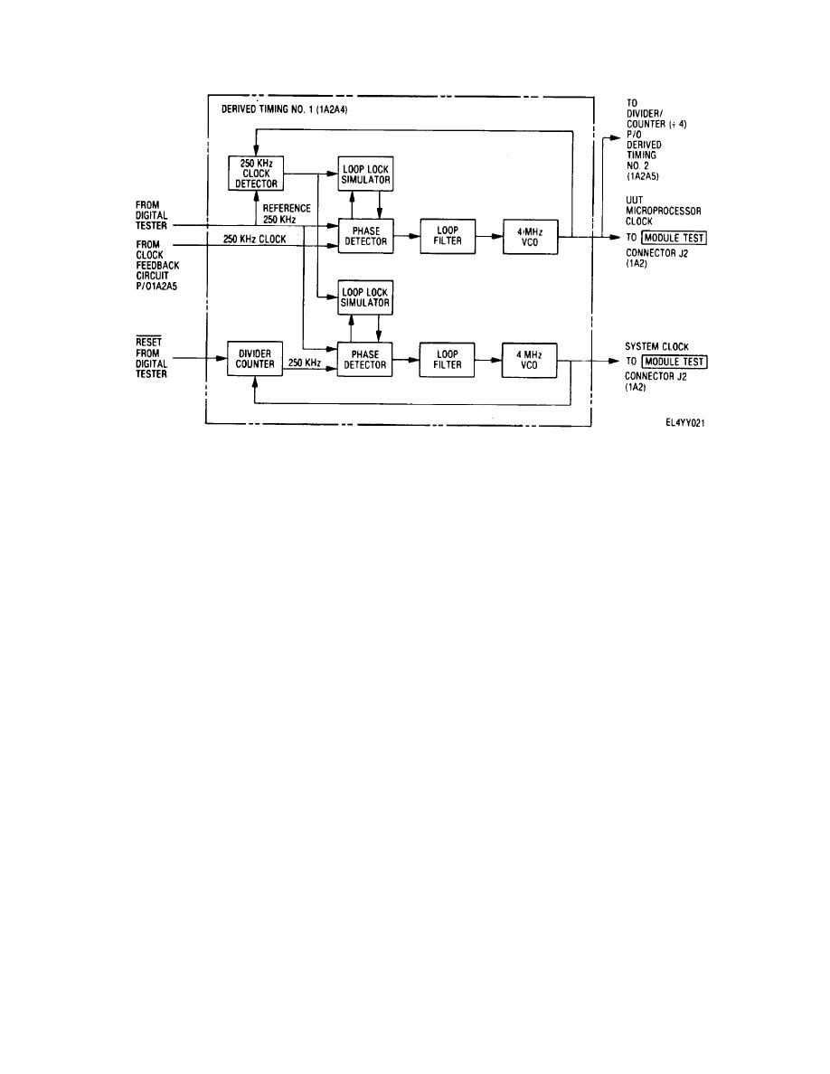
Figure 4-4. Phase-locked loop block diagram. |
|
||
| ||||||||||
|
|
 TM 11-6625-2937-13
Figure 4-4. Phase-locked loop block diagram.
d Panel Logic Functioning ft. 4-5).
(2) Mode select. The MODULE TEST position
(1) Power. Power from the digital tester and the
of MODE SELECT switch S2 (I A2) also provide MT
5 volt power supply (IA2A1) are APPLIED via the
ENC, MT DEC or MT STE signs to the select logic
MODULE TEST position of MODE SELECT switch S2
circuit, depending on the mode of operation selected.
(1A2) to the panel logic circuits . The switch selects one
MT ANC specifies module test encoder operation, MT
of the three modes of operation: ENC for encoder mode
DEC specifies module test decoder operation, and MT
of operation; DEC for decoder mode of operation; and
STE specifies module test special test equipment.
STE for special test equipment mode of operation.
When any one of these signals is applied to the select
Select one of three modes of operation provides the
logic circuit (lA2AI), MT ON signal is applied to ON
proper voltages for application to the power supply
indicator DS4 (1A2). The UT ON sin from the select
monitor (IA2AI) and the MODULE TEST connectors.
logic circuit (1A2Al) is applied to ON indicator DS2
When the encoder mode of operation (ENC) is Selected,
whenever the unit test decoder (UT DEC) or unit test
5 V and i 12 V are applied to the MODULE TEST
encoder (UT WC-) signals are applied from the UNIT
connectors and the power supply monitor (IA2Al). If the
TEST position of MODE SELECT switch S2 (1A2).
(3) BITE failure.
The write latch (1A2A1)
voltages are out of tolerance, the power supply monitor
provides the SHORT sign to fight SHORT indicator DS3
provides the FAIL control sin to the digital tester
(1A2). When the decoder mode of operation (DEC) or
whenever the control-interface unit fails a BITE test.
the special test equipment mode of operation STE) is
This signal is provided by the DATA BUS signal written
selected, + 5 V and 15 V are applied to the MODULE
into the write latch and by the LATCH 2 dock input. With
TEST connectors and the power supply monitor
the FAIL signal a-led to the digital tester, the normal
(1A2A1). Out of tolerance voltages light the SHORT
transition count of a programmed clock output from the
indicator DS3 (1A2). SYS RESET, which is used
digital tester is interrupted. Interrupting the normal
throughout the test set is apple from the power on reset
transition count causes the red FAIL indicator on the
circuit (IA2AI). The clock phased signal input .2 from the
digital tester to fight at the end of the test cycle. The
STE microprocessor (1A2A2) is t
to the power on
write latch also provides the MODE ERROR
which
reset circuit to activate SYS RESET.
fights MODE IN ERROR indicator DS5 (IA2).
4-11
|
|
Privacy Statement - Press Release - Copyright Information. - Contact Us |
