 |
|||
|
|
|||
|
Page Title:
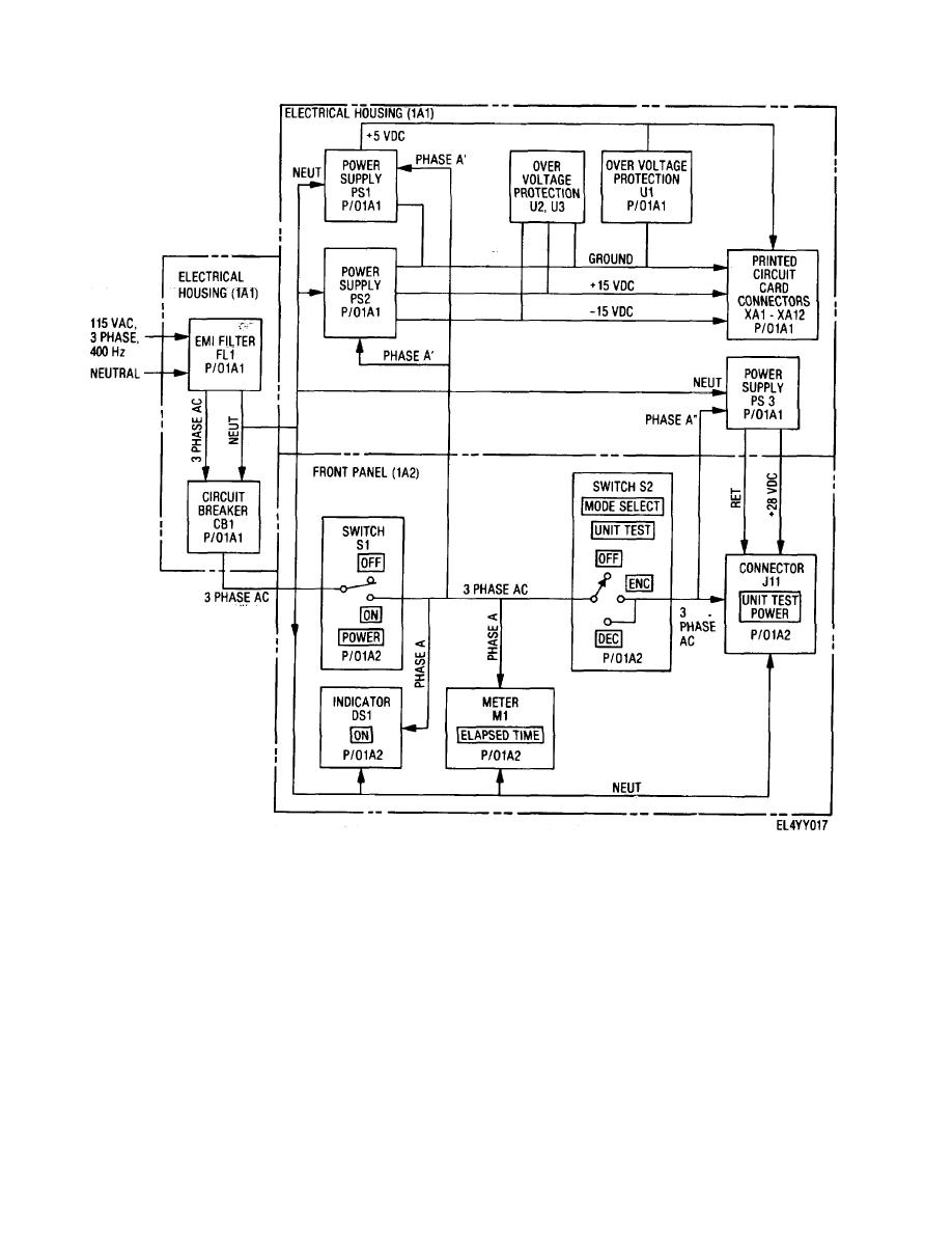
Figure 4-2. Control - interface unit overall block diagram (sheet 3 of 3) |
|
||
| ||||||||||
|
|
 TM 11-6625-2937-13
Figure 4-2. Control - interface unit overall block diagram (sheet 3 of 3)
(2) Mode verification Mode verification for the
TEST NUMBER are not in agreement with each other as
determined by the stored program in the mode
DC POWER and MODE SELECT switch S2 (1A2)
verification portion of STE program ROM I A2A3. TEST
positions is determined by that portion of the program in
NUMBER input from the digital tester is applied to 7-
the STE program read only memory POM) (IA2A3)
segment decoder (IA2AI) and STE MPU (1A2A2). The
which is used for mode verification when executed by the
BCD TEST NUMBER data is decoded by a 7-segment
STE MPU (IA2A2). STE MPU (1A2A2) is controlled by
decoder (IA2AI) which drives TEST NUMBER indicators
the mode verification portion of STE program ROM
DS7 through DS9 (IA2).
IA2A3 via the bidirectional DATA BUS and unidirectional
(3) Stimulus and transition counts. Stimulus in
ADDRESS BUS and CONTROL BUS. STE MPU 1A2A2
the form of DATA and CLOCK inputs from the digital
provides MODE ERROR SIGNAL to light MODE IN
tester are applied to MODULE TEST connectors JI, J3
ERROR indicator DS5 (I A2) if the MODE SELECT i,
and JS (STANDARD LOGIC). Dc power from the digital
which is input via the input port circuit (1A2A1), and the
tester
4-5
|
|
Privacy Statement - Press Release - Copyright Information. - Contact Us |
